Moore's Law and Tau Scaling, read side by side
Two papers about how chips should be expected to improve over time, separated by sixty-one years.
Gordon Moore's Cramming More Components onto Integrated Circuits appeared in Electronics, volume 38 number 8, on April 19, 1965. He Tingbo's A Time Scaling Theory for Multi-Layer Electronic Systems was posted to ChinaXiv on May 25, 2026, the same day she gave the ISCAS keynote in Shanghai under the title Semiconductor New Path: Exploration and Practice.
Most of the Chinese press has been reading He's paper either as a rebuttal of Moore or as a marketing exercise. Neither framing survives a direct read. What follows is a careful pass through both papers: what each one actually says, where they agree about the engineering problem, and where their answers diverge.
Moore, 1965
Moore's paper is six pages. The famous sentence is on the first one:
The complexity for minimum component costs has increased at a rate of roughly a factor of two per year ... Certainly over the short term this rate can be expected to continue, if not to increase. Over the longer term, the rate of increase is a bit more uncertain.
Three observations about that sentence are worth holding onto.
First, Moore was not predicting that transistor count would double every two years. He was predicting that complexity for minimum component costs would double. That is an economic claim, not a physical one. Every generation of chip has a sweet spot in the curve of cost-per-component; that sweet spot moves over time; Moore's bet was that it would move twofold per year.
The "minimum cost" framing was specific. Moore showed a U-shaped curve in his paper: at very low component counts a chip wastes silicon on overhead, and at very high counts yield falls fast enough that the cost-per-component rises again. The bottom of that U at any given year defines the economic sweet spot. Moore drew his actual line through five data points — the minimum-cost design at each year from 1959 through 1964 — and projected that line forward. The two-year cadence the industry later read into Moore's Law came from a 1975 revision, not the original paper. In the original, the doubling cadence was one year.
Second, Moore's time horizon was ten years. He wrote that by 1975 the economic optimum might be around 65,000 components per chip. Past that point his text is hedged. For a feel of how the original forecast played out: Intel's 8086, introduced in 1978, had about 29,000 transistors. The 8086 was three years late and roughly half the predicted count, which is closer to a ten-year industry forecast than most projections of that horizon ever come.
Third, Moore named the constraints he expected to run into: heat dissipation, manufacturing yield, the difficulty of getting clean electrical signals out of a dense circuit. He did not claim those problems were solved. He claimed they were tractable for the next decade.
What Moore defended in 1965 was modest and economic. It became something else later.
What "Moore's Law" became
Moore himself made the first revision. At IEDM 1975, in a talk titled Progress in Digital Integrated Electronics, he acknowledged the original yearly doubling had been "specific to the first decade" and proposed roughly a two-year cadence going forward. The shift was not anyone trying to save the law. It was Moore conceding that the easy density gains of the 1960s would not repeat at the same rate, and pricing in the constraints he had named ten years earlier.
The eighteen-month figure that floated around in the 1980s and 1990s was not Moore's. It came from David House at Intel, who combined Moore's density doubling with a separate prediction about clock speed improvements to get an aggregate eighteen-month performance cadence. By the time the cadence settled at two years for the public-facing "law," the original economic envelope around the prediction had been quietly dropped, and transistors-per-die became the standard scorecard on its own.
From the late 1990s onward the ITRS roadmap turned that cadence into a public commitment the whole industry coordinated against. Equipment vendors, fab capacity, EDA software, design libraries, customer roadmaps were all written assuming the cadence would hold. That coordination is what made Moore's Law work as long as it did. It is also why the slowdown after the 7nm node felt structural rather than incremental. The cadence was load-bearing on the whole industry's planning, not just on the physics of any one foundry.
Where Moore's prediction came under strain
Three things happened to Moore's economic curve from roughly 2005 onward.
Dennard scaling broke first. Robert Dennard's 1974 paper showed that if you shrink transistor dimensions by 1/k and supply voltage by 1/k together, power density stays constant while transistor density scales by k². That co-scaling let the industry push clock speeds up alongside density for nearly thirty years.
Around 65nm the voltage side stopped holding. To switch a transistor reliably you need supply voltage V_DD comfortably above the threshold voltage V_t. Think of V_DD as supply pressure and V_t as the cracking threshold of a closed valve. The geometric road keeps pushing V_DD down to save power, and you have to push V_t down with it to preserve switching headroom. But lowering V_t makes closed valves seep — sub-threshold leakage — and the rate rises exponentially with each further drop. Below roughly 1 V that seepage starts to dominate. At thin enough gate dielectric a second leakage path opens through the gate itself — gate-oxide leakage — that V_t scaling does not control. The net effect: you cannot scale V_DD down at the same rate as feature size without paying for it in static power, which compounds across billions of transistors and ends up dominating the power budget. The industry stopped trying around the 90/65nm node.
Once V_DD froze, dynamic power scales with clock frequency directly. Pushing the clock above roughly 3 GHz at the available cooling budget became uneconomic on the desktop and impossible on mobile. From 2005 onward, density gains had to be cashed out as more cores rather than faster cores, and most workloads either parallelized or stalled.
Lithography costs rose nonlinearly on top of that. EUV equipment moved past $200M per tool, and the mask layer count a leading-node process required grew faster than yield improvements could offset. The cost-per-transistor curve, which had bent downward through every previous node, began bending upward at 7nm and below. The engineering still worked; the economics increasingly did not.
The demand mix also changed. The most profitable workloads — large model training and inference — want memory bandwidth and interconnect throughput more than they want raw arithmetic density. A chip with more transistors that cannot feed them turns into idle silicon. None of this killed Moore's Law as a research metric. It killed it as the dominant industry economics. By 2020 you could find people inside TSMC and Intel describing the curve as "still continuing" while no longer claiming it set the pace of the field.
That is the historical setting He Tingbo's paper landed in.
He Tingbo, 2026
He Tingbo is a member of Huawei's board and the head of its semiconductor business. Her paper, A Time Scaling Theory for Multi-Layer Electronic Systems, opens with a direct statement about Moore's curve:
Over the past sixty years, the geometric scaling represented by Moore's Law drove continued progress in the semiconductor industry. However, this industry consensus has become difficult to sustain.
The paper proposes a different unit of optimization. Rather than transistor count per area, it proposes the characteristic time constant τ. The paper defines τ hierarchically across four layers:
τ_transistor, τ_circuit, τ_chip, and τ_system represent the time constants at the transistor, circuit, chip, and system layers respectively.
One operational meaning per layer, as the paper spells out:
- Device layer: shorten the intrinsic switching delay of the transistor itself.
- Circuit layer: shorten the RC propagation delay along signal paths.
- Chip layer: optimize the latency between compute and memory access.
- System layer: shorten end-to-end message passing and synchronization time.
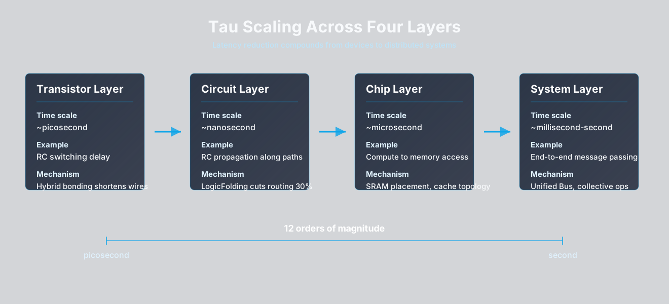
The paper is explicit that the four layers are not parallel projects. Any τ optimization at any layer, the paper says, "must propagate to the system layer to yield real value." Layer-local wins that do not reach the system level do not count.
A worked example: LogicFolding
The concrete mechanism the paper attaches to its first commercial proof point is LogicFolding, the technique used in Kirin 2026.
A traditional planar SoC lays out digital, analog and memory blocks on a single active layer, with metal interconnect stacked above. Two transistors that need to communicate are connected by metal traces whose length is set by where they sit on the floor plan. As designs grow, the wire length between communicating blocks dominates RC delay, and the layout has to grow clock buffers and clock-tree branches to compensate. The τ at the circuit layer is, in large part, that wire length.
LogicFolding splits digital, analog and SRAM into independently optimized active layers and bonds them with hybrid bonding: direct copper-to-copper interconnect at sub-micron pitch, replacing the traditional micro-bump interconnect with its 10–40 µm pitch limits. At roughly 1 µm hybrid-bonding pitch, vertical layer-to-layer links become the dominant geometric quantity rather than horizontal in-plane routing. Two communicating blocks can sit directly above each other rather than across the die. Routing length drops; clock buffers needed to drive long traces go away; SRAM access frequency rises because the path to the compute layer no longer crosses the long planar route.
That mechanism is what makes the 55% density gain at the same process node possible. It is not a violation of geometric scaling. Feature size has not changed. It is a change in which geometric dimension carries the density. Vertical instead of in-plane. Building up instead of out, in the most literal sense — same footprint, more floors.
The math, side by side
Both papers can be reduced to a single generational equation.
Moore's, in modern notation:
N(t) = N₀ · 2^(t/T)T ≈ 1 year in the 1965 paper, revised by Moore himself to T ≈ 2 years in 1975.
He's, from her paper:
τ_(n+1) = τ_n / αα is application-conditional: roughly 1.3 for mobile, 1.5 for autonomous driving, and up to 10 for AI workloads.
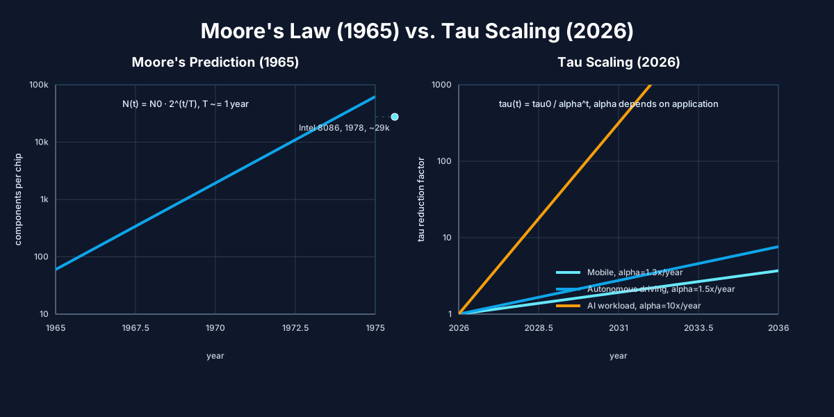
Two things in those equations are worth noticing.
First, the structure is the same. Both are exponential in time with a single application-or-period-specific compounding factor. Both place that factor on production data rather than on theory.
Second, the moving direction is reversed. Moore's quantity is something you want to maximize — transistor count at minimum cost. He's quantity is something you want to minimize — time. Functionally both are improvements at a compounding rate. Rhetorically "transistors went up" is easier to communicate than "time went down by the same factor," which is part of why Moore's Law became a slogan and τ scaling probably will not.
Reading α correctly
The α figures are where the paper most often gets misread. The full sentence:
The scaling factor α is not a universal constant; it depends on application. Mass production experience to date shows α of approximately 1.3× per year for power-constrained mobile devices, 1.5× per year for safety-critical autonomous driving systems, and up to 10× per year for AI workloads.
The substantive claim is that α depends on workload. That is a substantially weaker claim than "10× per year for AI" taken on its own, which is how the Chinese press has been reproducing it. The paper does not claim a single τ curve across the industry. It claims the curve is application-conditional, and the AI number is the largest because AI workloads have the most accumulated headroom in data movement and scheduling.
The position toward Moore's Law is also explicit:
Geometric scaling becomes one of multiple techniques for reducing τ, no longer the sole path. This principle is called τ scaling.
Worth pausing here. The paper does call τ scaling the successor framework, and the move is real. The narrower point is that it keeps geometric scaling inside that framework as one technique among several rather than the sole path, and shifts the optimization target from feature size to τ. That framing is more modest than most of the recent press coverage.
Where the two papers agree
Both papers anchor their cadence in shipped product rather than physics alone. Moore drew his curve through cost-per-component data from minimum-cost designs in 1959 through 1964. He's α values are quoted as "mass production experience to date," meaning improvement rates actually achieved on shipped silicon. Neither paper is a pure physical scaling law; both stake their credibility on what shipping product has demonstrated so far.
Both papers commit to a cadence. Moore's was a single annual factor of two for ten years, later revised by Moore himself. He's is application-specific compounding, with no fixed horizon, but the structure is the same: each generation gets you a definite factor closer to the limit.
Both papers identify the binding constraint of their era as a system constraint, not a transistor constraint. Moore worried about heat dissipation, yield, and signal integrity at the package and circuit level. He worries about end-to-end signal time across chip, package, and rack. Both papers say, in their respective vocabularies, that the limit lives outside the transistor.
Where they part
The metric is different, and that pulls the rest along with it.
Moore's metric is component count at minimum cost. The optimization variable is feature size. The lithography roadmap is the central lever. Once a leading-node fab is too expensive to build, the curve bends.
He's metric is τ at a chosen layer. The optimization variables are packaging, layout, interconnect, and software-level scheduling, with feature size as one input among several. A node freeze does not immediately kill τ scaling, because most of the levers run on layers above lithography.
That is the genuine engineering distinction, and it does not depend on either author's geopolitics. Moore wrote in a country with leading-edge lithography access; He wrote in a country without it. The metric each one defended is the one that survives best under their respective constraints. That observation is consistent with both papers being good engineering, rather than either one being marketing.
There is one structural difference that matters more than the metric itself. Moore's Law became "the law" not because Moore wrote a paper, but because the entire industry coordinated against it. The ITRS roadmap from 1998 onward was an explicit consensus document signed by SIA, JEITA, KSIA, ESIA, and TSIA, and the foundries, EDA vendors, equipment makers, and IP companies paced their roadmaps to it for two decades. That consensus is what made the cadence load-bearing on the whole industry, not just on any one foundry's process.
τ scaling has no equivalent body. As of 2026 it is one vendor's framework. TSMC, Samsung, and Intel have access to leading-edge lithography Huawei does not, so they have less incentive to adopt a metric where lithography is one of several levers rather than the central one. The most likely outcome is that τ scaling stays a Huawei-internal organizing principle that produces results visible in Huawei products, without becoming the kind of industry-coordinated cadence Moore's Law was. That is a real limitation. It is not the same thing as a flawed paper.
A harder question is whether τ as a single metric actually unifies the four layers. The paper claims it does. The math the paper supplies, with τ as the composition of layer-wise time constants, is closer to a bookkeeping convention than to a unified theory. Twelve orders of magnitude is a wide span — a picosecond is to a second what a second is to about thirty thousand years. Whether that range really yields to the same kind of optimization mindset is not yet visible from a single paper.
The testable parts of He's paper
A short list of claims that will resolve themselves over the next few years.
α of 1.3× per year for mobile is testable starting in Q4 2026, when Kirin 2026 phones reach independent benchmarks. Sustained performance over Kirin 9020 is the closest user-visible proxy for an integrated τ reduction across the four layers, because the paper's +41% SoC perf/W gain should compound into a visible sustained-perf delta there. If independent benchmarks land well under 30%, the 1.3× production-experience number was generous.
The 100-nanosecond cross-rack remote access latency is testable once CloudMatrix 384 deployments are profiled at near-saturating utilization with public methodology. The paper's number is roughly a five-hundred-fold improvement on typical microsecond-class numbers. Checking it at realistic LLM training and inference loads is the right test.
The 2031 target of 1.4 nm-equivalent transistor density is checkable on a continuous schedule. It does not need to land precisely in 2031 to count as supporting the paper. A slip of three or more years would count against it.
α of 10× per year for AI workloads is the noisiest claim and the hardest to evaluate. AI workload economics are changing fast enough that even reasonable improvement rates will look like step changes for a while. The number is plausible as a description of the past few years. As a forward-looking forecast it deserves a wider error bar than the paper gives it.
What I think after reading both
Moore's 1965 paper is a careful economic observation with a ten-year forecast and named constraints. He's 2026 paper is a careful engineering observation with an application-conditional forecast, named constraints, and a multi-decade roadmap target. Both are more modest in their text than they have been in their reception.
The serious thing in He's paper is the choice of metric, not the slogan. Optimizing τ rather than feature size is a defensible engineering decision in 2026, and the four-layer decomposition gives a working vocabulary for parts of the problem the Moore-Law cadence had stopped addressing. Whether that vocabulary survives outside Huawei's vertically integrated stack is the open question. My guess is partly. The device-layer and circuit-layer work generalizes — hybrid bonding and LogicFolding-class techniques are visible in TSMC's SoIC and Intel's Foveros direct-bond stacking, just under different names. The system-layer work depends on owning the interconnect, and there τ scaling will probably stay a Huawei-internal framework with Huawei-specific numbers.
The press has compressed the paper to a single number: 55% density without a new node. That is one product, one application class, one data point. It is also a real number. The right reading is neither dismissing it as marketing nor treating it as a forecast for the whole industry. It is one validation of a wider framework whose other validations are still ahead, and the next few that come in will tell you most of what the paper is actually worth.
References
- Moore, G. E. Cramming More Components onto Integrated Circuits. Electronics, Vol. 38, No. 8, April 19, 1965, pp. 114–117. PDF
- Moore, G. E. Progress in Digital Integrated Electronics. IEDM Technical Digest, 1975, pp. 11–13.
- Dennard, R. H., Gaensslen, F. H., Yu, H.-N., Rideout, V. L., Bassous, E., & LeBlanc, A. R. Design of Ion-Implanted MOSFETs with Very Small Physical Dimensions. IEEE Journal of Solid-State Circuits, Vol. 9, No. 5, October 1974, pp. 256–268.
- He, T. A Time Scaling Theory for Multi-Layer Electronic Systems. ChinaXiv preprint, May 25, 2026.
- He, T. Semiconductor New Path: Exploration and Practice. Keynote, IEEE International Symposium on Circuits and Systems (ISCAS), Shanghai, May 25, 2026.
- Huawei. HUAWEI Presents the Tau (τ) Scaling Law, Enabling Breakthroughs in Transistor Density and System Performance. Press release, May 25, 2026. Link